Finished projects
This a joint project of Ovidiu Popa and Edmond Stuart. As a matter of fact, Ovidiu did most of the work, as he designed the
output stage, built the amplifier, including the power supply and auxiliary circuits and did all the measurements. Edmond
designed only the front end did the simulations.
Schematics, photographs, measurement results etc. can be found on our dedicated websites here or here. Also see the PGP
thread of www.diyaudio.com and here for some listening tests.
Below some additional information about NDFL and the design rules.
PGP (Pretty Good Power amp), additional information.
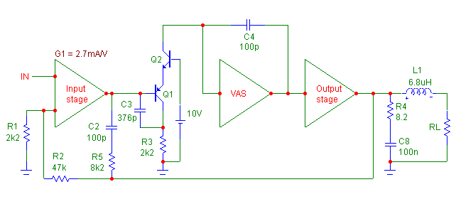
Fig.3. Simplified NDFL stage used in the front end of the PGP amplifier (current sources etc. not shown).
This one differs not only in that it is fully symmetrical, but also the feedback paths have been changed. Now the lag
compensation (C2 and R4) is applied between the emitters of Q3 and Q4 and the inverting input of the preceding stage. Also,
the nested feedback (as in fig.2, C2 and R5) has moved to the inverting input (C1 and R3). Strictly speaking, this is no longer a
nested feedback, as it leads to the same input as used by the global feedback (R2). Nevertheless, the behaviour of this
topology is equal to the previous circuit. An important feature of this arrangement is the low requirement of drive current of the
input stage. As a result, the DIM and TIM is virtual zero.
New design rules
The design rules for this case are completely different. The gain of the global feedback loop (around R2), for example, is
(almost) independent of the trans-conductance of the input stage.
Here are the cookbook design rules:
1. Choose R1 and R2 to set the closed loop gain as usual, preferable low values to decrease the Johnson noise.
2. Choose The Miller compensation cap. This one determines the unity gain frequency of the global feedback loop. Usually, this
value lies between 0.5 and 2MHz. A choice is mainly governed by the speed of the output stage. In the PGP amp it is set at
700kHz and corresponds to a time constant Tx of about 220ns.
Since Tx = R2 * ( C3a + C3b ) * Rp / ( R4 + Rp ) and Rp = R5 || R6
then: C3a + C3b = Tx * ( R4 + Rp ) / ( R2 * Rp ) = 220n * ( 270 + 270 ) / ( 2k7 * 270 ) = 163pF
If C3a = C3b = 82pF, then Tx = 221ns.
3. Select a convenient value for R6, but at least 3 times higher than R1. R6 corresponds to the parallel value of R32 and R33 in
the simulation schematic. Together with the Zener voltage of D3, they determine the quiescent current of the NDFL stage, which
is set at 7mA. So R32= R33= 560, thus R6 = 280 Ohm.
4. To keep the emitter voltages of the NDFL stage at the same level as the input voltage, this stage is bootstrapped by means of
R5, so set R5 = R6 * R2 / R1 and calculate Rp = R5 // R6
5. Although value of R4 is not critical, it is convenient to set this value equal to Rp ( then Tx = R2 * C3a / R4 )
The leading time-constant is defined by Tf = R3 * C1
and the lagging time constant by Tl = ( R4 + Rp ) * C2
C1 corresponds with C3 in the simulation schematic, and C2 with C10 and C11 in parallel.
Tf and Tl should not only made equal to Tx, just as in the previous example, but also R3 should be equal to R2, as the lead
compensation is connected to the same input as the global feedback network.
Substituting the actual used values we get:
Tf = 2k7 * 82pF = 221ns
Tl = ( 270 + 270 ) * 440pF = 237nsested feedback (as in fig.2, C2 and R5) has moved to the inverting input (C1 and R3). Strictly
speaking, this is no longer a nested feedback, as it leads to the same input as used by the global feedback (R2). Nevertheless,
the behaviour of this topology is equal to the previous circuit. An important feature of this arrangement is the low requirement of
drive current of the input stage. As a result, the DIM and TIM is virtual zero.
Tweaking
In the next figure the annotation from the simulation schematic is used.
As one can see, miscellaneous capacitors and resistors are added. However they dont form part of the NDFL circuitry. Rather,
they increase the phase margin of the internal loops around the input stage and the VAS respectively.
Regarding R2, one should notice that this one is subjected to the full output voltage and it dissipates a relative large amount of
power (~ 0.5W) . To ease sufficient power rating in a future update, it might be beneficial to put R2 and R3 in series and (of
course) adjust the values of R2, R3 and C1 accordingly, see figure below.


As mentioned before, the clipping and recovery properties of a NDFL amplifier are rather poor, that is, without further
measures. The main reason for this misbehavior stems from the NDFL capacitors (C10 and C11), which are heavily
overcharged during clipping and the fact that it takes too much time to discharge them at the onset of recovery. So the
question is how to prevent overcharging. Simply limiting the capacitor voltage is not only troublesome but also
compromises the slew rate. This leaves one option: limiting the input signal.
In the PGP amplifier this is achieved by means of an additional feedback loop from the VAS output (Q31) back to the
inverting input (Q7 and Q8). Normally, increasing the loop gain would easily lead to instabilities, as the phase margin
becomes too small. However, during clipping, the incremental gain of the main feedback loop gets very low. So, if one
can manage that only under these circumstances the auxiliary feedback loop comes into action, one major source of
instability has been eliminated.
Indeed, this is possible, just by duplicating the current through the Baker clamp and feeding this 'copy' back to inverting
input (see Q27a, D5 and R25). This scheme ensures that additional feedback only takes place if the gain of VAS
already has been reduced to avoid oscillations. The reader may wonder why this feedback is led to the node C10-C11,
instead of directly to the inverting input. The reason is quite simple: using this node provides a lead-lag compensation
and improves the phase margin, Moreover, it is 'free', as no additional components are needed.
As a finishing touch, D5 and R26 are added in order to mask leakage or parasitic currents from Q27a.

Fig. 5. Red lines show the signal path of the clamp. Click here to see complete schematic.
Fig. 6. Gain and phase response of the nested clamp at various overdrive voltages
The roots of Nested Differentiating Feedback Loops (NDFL)
In the late seventies, Edward. M. Cherry invented the technique of NDFL (U S Patent 4243943) Despite its simplicity, the
improvement in terms of distortion reduction is an order of magnitude. Amazingly, this technique has never found widespread
use in audio amplifiers. Why? I only can guess. One reason could be that he confused the reader of his paper[1] by combining
this technique with two other tricks: enclosing the output stage in the Miller compensation loop (OMC) and using a tap on the
Zobel network for global feedback. Not everyone, I suppose, will be charmed by this magic. Another reason might be the poor
clipping and recovery properties and, admittedly, solving this issue is not an easy task. Happily we were able to tackle this
problem adequately, probably a first in the history of audio engineering (see below, nested clamp).
Starting with his original implementation I will show in the next picture how it can be converted to a more commonly topology,
that is, just a pure resistive divider for global feedback.
Fig. 1. Cherrys original implementation.
Summary of the design rules
There are three distinctive time constants
1. Tx, which defines the gain and unity crossover frequency of the global feedback loop.
Tx = C4 / ( G1 * B ) = 100p / ( 2.7m * 0.0447 ) = 828ns
Where G1 = trans-conductance of the input stage and B = R1 / ( R1 + R2 )
2. Tl, which defines the amount of lag compensation of the NDFL stage.
Tl = R3 * C3 = 390p * 2.2k = 858ns
3. Tf, which defines the defines the amount of lead compensation of the nested feedback loop
Tf = R2 * C1 = 12p * 47k = 564ns
Now Cherry stated that the response can be made phase linear by choosing:
Tl = Tx and Tf = (sqrt(3) -1) * Tx = 606ns.
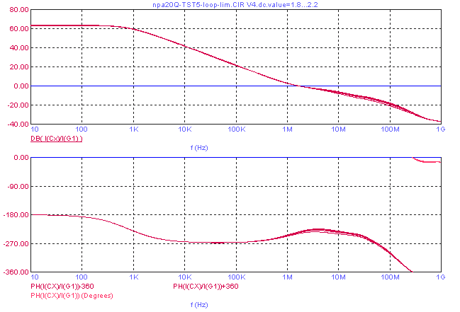
First, notice that C4 is a little bit too high and should actually be 376pF and C1 is a little bit too low and should be 12.9pF.
Second, maybe Cherry is right regarding a linear phase response. Again, Im not charmed by this approach, giving an
overshoot of 14%! So I prefer that Tf is also set equal to Tx, because in this case the response is critical damped, and no
overshoot will occur. Now lets remove the tap, revert to the traditional Miller compensation and set Tf = Tx. Then the equivalent
circuit looks like this:
Fig. 2. Modified version of Cherrys NDFL AMP
The new design rules are: Tf = Tl = Tx, where Tf = C2 * R5 , Tl = C3 * R3 and Tx is defined as above. It should be noted that
the amount of overshoot is mainly influenced by a mismatch of the time-constants of C2 and R5 respectively C3 and R3, while
Tx has a strong impact on the rise and fall time. BTW, Q1 and Q2 may look funny, although its derived from the so called high
speed Rush amp. Of course, many other implementation are possible, but lets jump directly to the topology as used in the
front-end of the PGP amp.
References:
[1] E.M.Cherry, Nested Differentiating Feedback Loops in Simple Audio Amplifiers, J. Audio Eng. Soc.,Vol.30,No.5, 1982 May,
pp. 295-305.
[2] R.J. Mitchel, "Nested Velocity Feedback Control",
http://www.personal.reading.ac.uk/~shsmchlr/miscfile/CS2007RJMitchell.pdf
Fig.4. Tweaked, but still simplified NDFL stage used in the front end.